Day 54
It has been a busy couple of days and my head hasn't really been in the game so no real post today but the announcement that I am in fact switching to 1 day a week posts from here on out Wednesday will be the day so. More to come then and I will be back on track. There is still an excitement in me about this project but I need to temper things to a slow burn to account for the duration this project will take. Wednesday we will be breaking down the machine language of professor Porter's design and my proposed changes to it. and from there likely a walk through of his control circuits.
Saturday, March 26, 2016
Wednesday, March 23, 2016
Finally the answer I've been seeking
Day 51
Finally I think I've hit on what I've been missing for the overall function of this machine. That is the good news, the bad news is it's the part even professor Porter says figure it out for yourself on with no real parachute. Oddly enough this fills me with excitement rather then dread.
The finite state machine feeds into the combinational logic which is what decodes the instruction from the memory to the necessary control lines and timing instructions to preform the proper sequences in order. This may be a limiting factor while I wrap my head around this but in the day or so I have been working through it I am already seeing how it will work and what it may require for the more advanced designs I'd like to include in my design. Essentially each instruction you want to include has to have it's own physical decoding this is straightforward enough but the trouble comes in with the added function codes I would like to add it may require an upgrade to a 16 bit instruction system.
This genuinely is the break I have been searching for years for the single key my little mind has refused to understand to break the barrier between what you want to do and what the how the computer determines what steps to take to accomplish that goal. It is also 1 of the primary missions of this project to truly grasp how we went from instructions to execution in a computer I am beyond excited about what this means and cannot wait to study this further. I will need several days to process what this means for this project in particular but I can see from here that it will make things fall into place much better I am already grasping the function of the finite state machine and all of its ancillary components much more fully now.
The instruction calls are based on 8 bit instructions that for obvious reasons cannot repeat. they are called in the order they were indexed based on a 16 bit memory address this address is usually incremented to the next instruction but there are several instructions which will either temporarily or permanently jump to a completely different instruction address. This system is overall nearly identical to the machine language of modern computers with some differences in execution. These 8 bit instructions are the limit to the bus size for my redesign the positive here is if I include the constant function separately like I want to then this will open up several new instruction sets as there is an instant instruction which is the same as a constant but instead of having the constant loaded from a register or switches it is loaded in as 5 bits of the instruction. The design of this instruction set will require quite a bit of work, checking and re checking to make sure there are no duplicates. If all else fails then I will have to move to a 16 bit data bus and expand the whole computer or rework the intire instruction system. Neither is out of the question though fully re working the instruction system would likely be much cheaper though not very fast as I would be starting from scratch in this lesser understood area with professor Porter's original design as only a road map. My mind is saying it may be cleaner and easier to build the instruction set up to a larger number of bits that will allow for not only a more robust instruction set but a slightly cleaner execution though only fiddling with this idea would be able to tell if it could lead to fewer physical components in the build.
I have also made a decision on the physical layout of my computer. The various sub assemblies will be housed similarly to the clock circuit. On their own boards or plexi inserts just like professor porters system but each module will plug into the backing plane with a physical connector which will allow for easy removal and repair of faulty modules. Though I do not foresee this having a high degree of usage I would still like to think of the poor servicing guy (me) when something does inevitably break or blow smoke on me. These modules will be attached to their faceplates and the faceplates will be cut to fit the area allotted them in the cabinet.
This is a short update because of these revelations but Saturday will be jam packed with information I am sure of that. I won't venture what direction I'm going to end up chasing this in yet. But we shall see then.
Saturday, March 19, 2016
Finite state machine is a tough nut to crack
Day 47
Professor Porter goes into great detail about how the finite state machine works and it's theory of operation. However he does not show a full blown schematic, but there is a layout in the various downloaded image files, for this vital portion of the computer. He somewhat seems to leave much of this area up to you to figure out. However, this is the some of the truly uncharted territory for me I understand the abstract of this system but cannot quite wrap my brain around the full function of this. I understand that it is essentially breaking out the clock pulses so that each individual pulse can control the specific portion of the computer it has to but the underlying control structure it orchestrates is eluding me for the moment. This lack of understanding is somewhat exacerbated by professor Porter's desire that those control systems be figured out by the student as well. This is an area I need to study more and shows that perhaps I should go back and try to better understand how all of these functions are executed. This is the plan starting with today's post.
So instead of killing myself by jumping around in the paper any further I am just going to mosey on from where I left off with the adder. This brings us to the zero detect circuit it's function is very simple it's use, however is not immediately apparent to my eye unless it can be used to call a halt or perhaps if factoring a number but I am not sure beyond those 2 cases hopefully it's need will be demonstrated in the future. The sign bit is discussed next and it is simply represented by the most significant bit on the bus this means that instead of a full 8 bit word we a technically only working with 7 bits for numbers and 1 bit for sign. This is actually somewhat confusing as you look through the paperwork as in some diagrams professor Porter has the sign bit broken out from the ALU output but in many of the block diagrams but in the reference materials and schematics it is nowhere to be seen so this is how I ended up drawing this conclusion. For the ALU functions this makes sense as any function performed on this bit to compare it to the sign bit on the other register will result the mathematically proper answer. the only issue with it I have is if a number carry's over to the 8th bit it will give an incorrect answer, but these kind of non error errors can be seen in many older systems and in the design history of several programming languages. It is simply misleading in various diagrams and the like.
The 3 to 8 decoder shown in professor Porter's design has been replaced in mine by the 4 to 16 design which is a simple extension of his principals. This is done to accommodate the added functions I would like to include in my build. So far we have added a right shift but I am considering adding a subtract function if it is plausible. Other considerations so far are a constant (not necessarily as part of the decoders function), A NOT function for the "C" register, a NAND function, and finally a potential multiplication function. As these ideas represent only 4 or 5 additions to the decoder they would be no problem for that end, the limiting factor will be my desire to expand the ALU and by extension the part count. This does leave me open to adding other functions that may use unused portions of the existing system or combining some functions like in the logic block. For instance the NOT "C" function or the NAND function could be incorporated into the existing logic block and as such would add very little overhead but almost all of the other functions will add to the parts count by at least 10 relays. If I attempt this less expensive single or double pole relays may find their way into the project. Many portions of this are still up in the air. Another modification I will be making to the decoder is the change of the "000" input going from ADD to "Not Used" this is a clearly stated flaw in professor Porter's design and 1 that I will build out of my design. the simple truth to this is that it takes no effort to send that "000" down the line which means that any time the system does not need the ALU to output then it needs only cut power from the decoder. The original design used "111" as the "Not Used" which meant that power to the decoder could not be cut unless you wanted to ADD.
Wednesday we will be talking about the overall system architecture as a warm up for breaking down those control systems and what they entail. I will be focusing on the various registers and what their functions are in the operation of the computer.
Wednesday, March 16, 2016
Adder unit, the end of the functions
Day 43
The adder is discussed in some detail in a few places but it's design is identical to that of Konrad Zuse from the 1941 relay computer he built. I have included a Fritzing diagram of the single bit and the full 8 bit chain in the Google Drive folder I have only done a screencap of the single bit as to zoom out enough to see the full chain of adders makes it virtually useless as an aid.
On top of the discussion in Harry's paper on the he also points us to a Java applet demonstrating the adders function. I have not jumped through the hoops necessary to get this to work on my computer as I keep Java on a very tight leash for security's sake, but it looks fascinating. Both give a decent rundown of the history of the adder though the Java page gives a bit more detail I will not attempt to mess with what seems to me so succinct and as such will be following Harry's lead and simply copying this full adder over to my design, which is even used in the RC2 design unaltered. The other function of this circuit is incrementing this function will take Bin and output a +1 to it instead of adding it to Cin this is accomplished by inputting a 1 to the Carry in on the 0 bit a a simple control circuit for these functions is shown in the RC2 plans and I will likely be basing my design on it.
This is the last of the functional portion of our design from here we get into the program counter and the memory and the various control circuits and putting all of these circuits together with those controls shows the 1 major flaw in this design besides speed. That is inefficiency the adder all of the logic functions and the shift operations all happen regardless of weather or not they are needed we simply select the 1 we want to go out onto the bus this design while simple is very inefficient in power consumption and in the lack of ability to multitask. In modern computers these functions can all be happening to different sets of numbers simultaneously or nearly as such. this is called multi-threading and it drastically helps to increase speed of computing as it means 2 or more calculations are happening at 1 time, which effectively doubles, triples, or quadruples output speeds. This effect could be performed in our design but it would come at the cost of greatly increased complexity and cost several new registers would need to be added to the design to store the numbers as well as a drastic overhaul of the control and mode selection system and the addition of at least 1 more bus or a widening of the existing bus. While these changes would be fun to make and I am not throwing them aside for a long term project the lack of real world use cases for this device limit even my desire to chase that rabbit. For now I think this system will suffice for my purposes.
Next I do believe some design and discussion on the finite state machine will be in order. This will start giving structure to the underlying control systems we will be building in later. Then after or during that we will start our mock ups of the various portions of the system we have already discussed. I am working on a build up board design to make the build ups go more smoothly and allow us to see each circuit in detail.
Saturday, March 12, 2016
Explaining motives in depth
Day 39
Ok first an apology for the massive divergence but I think it's a necessary one. A few program notes before I get to the meat and potatoes of this post.I am breaking things down a bit I have a few other ideas I want to get started on that don't involve this project and as such I'm cutting out the Monday posts to this blog. The aim here is to educate and explain and the pressure of 3 posts a week for a project setup to be this long term is a hard self goal so we're going to try 2 a week for a while and see if that not only improves quality but coherence of things. So from now on Wednesday and Saturday for posts and hopefully a new announcement soon. On the physical build the clock circuit will be finished soon but after it is finished I have a Christmas gift I should have finished first to get back to then after that is done we will resume with the various test builds.
As an explanation for this post I was chatting with my girlfriend the other night about this particular project and I was asked about not only the function of this computer but the purpose and use for it as well. The 2 answers kind of go hand in hand so I'm going to attempt to break it all down in this 1 post.
I am an unabashed geek there is no denying it and I wouldn't dare insult anyone's intellect by trying to. This fact leads to several assumptions some right and some not so much. First I love tech and all of it's many forms I have an intrinsic knowledge of how electronics function this makes me a superb troubleshooter. Unfortunately it tends to lend credence to people thinking I know how these things work on a deep level, I do not, usually. When it comes to computers especially I am quite knowledgeable about how the OS works and how to sort out problems like that as well, I also have the aforementioned tech skill which helps find physical issues quickly. These 2 skills make for a great repair man but that does not require a knowledge of how a PC thinks and preforms it's functions. More importantly given the way my brain works this lack of understanding leads to a disconnect between the hardware of the computer and it's software. I get the abstract of it all but when I try to apply this knowledge nothing makes sense and I quickly lose patience with the situation. I have broken down much of this project into parts that I understand fully, parts I half get, and parts I am completely lost on. The only parts I'm completely lost on are the actual programming of this beast the physical parts all make at least some level of sense and I am 100% certain will all make total sense once I take the time to break them down and model them. So goal #1 is to better understand how modern computers work and use that knowledge to boost my ability to code and problem solve for the machine.
Goal #2 goes back to the unabashed geek thing I love tech and historical tech like this relay computer or the PDP-8 from DEC or even the DOS like DEC system I work with at work is utterly fascinating. The relay computer is not the first computer ever built but it was an important milestone in the road to the transistor and also within reach of a hobbyist such as myself affording and building. Relays are readily available and are largely unchanged in function if not design from that time, this means that any computer I build in this manner will be very similar to what came before. Historically speaking while this uses no semiconductors or any of their direct precedents (Vacuum tubes)it still functions in nearly the same manner as a modern PC's processor. The series of registers and functions are all largely unchanged in ability though the scale is simultaneously much larger and much smaller. So goal #2 is simply to have built a piece of history.
Goal #3 is short and sweet. This is a project to do with my kids who have both shown at least a mild interest in the topic. The knowledge they gain from this can easily help them in their lives from a better understanding of mathematics to problem solving to an early exposure to real engineering. Plus they can make it make lots of noise. That's about it for goals, there are more but they're minor.
Now as for a purpose for this computer that's a bit more abstract as it cannot do things a modern PC can. What it can do is math and in a consistent and loud manner. So doesn't this make it a glorified calculator? Why yes, yes it does just like your iPhone or DROID or Dell. The difference is in the learning and teaching ability with this glorified calculator. Not only am I learning something but see goal #3. This machine can be rolled out for whatever special occasion calls for it or more likely will simply become 1 of my trophy's of geekdom. It will likely be stored until I get a place of my own and then it will be placed on display wherever I put things like that. It can be programmed to preform many complex functions but really any everyday use of it is impractical and as such any question about it's use is like asking for an explanation as to why children play. There is no point or use beyond the education of it.
Now that I have that out of the way we can get to the explanation of what this all does. Obviously this is a computer but not like what many people carry around or have sitting in their homes. This was before programming languages made it easy to preform complex multi step functions with just a few words. This is like trying to use a modern computer without the mother board, monitor, keyboard, and mouse. The computer I am building here is what functionally happens all on the CPU's chipset in a modern PC. Most people have experience typing things into a computer and getting information back but the part they miss is loads of other people spent boatloads of time making the system work that way. Essentially a modern computer is a translator for a translator for the CPU and you to communicate. Most programs break your inputs like mouse clicks and keystrokes into some type of bytecode this is a numerical representation of what you are requesting the kernel of the processor turns that bytecode into the logical 1's and 0's the CPU can actually work with.
Those 1's and 0's are what we are working with in the relay computer. Instead of having a program put those 1's and 0's in for us we put them in manually using switches. The switches help us preload the computer with everything it needs from the instructions to preform the program to the starting inputs of the program itself. these inputs are made with the clock off and it is either manually cycled to allow for the next input or set to run to allow the computer begin its automated calculation of whatever program was inputted. This whole process is done either automatically by modern computers or prewritten by the program designers. In the case of prewritten instructions they are usually written in some higher programming language like C++ or Java which then has to be compiled into bytecode that the CPU can then translate into the instructions for the CPU to preform. This double translation is done to make programming more accessible the higher languages are more human readable and allows us to succinctly preform complex calculations. Some programmers write in machine language which is essentially talking directly to the kernel, this has a few advantages. First super lightweight code machine language has virtually no overhead and as such it is really easy to drastically reduce file size. Also it tends to run much faster. The downsides are that it is truly difficult to master comparatively to other languages. It is also so powerful that small mistakes can cause massive problems from system crashes to security vulnerabilities. It is also highly specific to the system it is on while Java can be compiled for a Mac or PC or Android without trouble each has its own machine language to be learned. We will be working with our own machine language for this build as the instruction set will be used to directly interface with the various functions we can preform.
I hope this has been as enlightening to you as it has been clarifying to me in where we are and where we are headed.
Wednesday, March 9, 2016
ALU logic functions
Day 36
Today we'll be breaking down the logic block of the ALU, but first a word on the build I still haven't gotten the clock finished though not due to any real difficulty other than a lack of time. should be getting it finished soon but no distinct timeline as of yet.
The logic block contains 2 inputs in the form of the B & C registers and preforms several functions on those inputs simultaneously the only thing that determines what is gated onto the bus is the enable circuits for each function. each bit of the logic block contains 2 relays using a total of 16 relays to preform the NOT "B", AND, OR , and XOR functions. There is an unused switch in the logic block and I may put it to use as a NOT "C" function to further reduce cycle counts for functions that may need to NOT 2 numbers back to back, but I am unsure if it has any real benefit yet so for now it is tabled.
The NOT function takes the input from the B register which is
inputted to the coil and simply outputs the opposite. Thus if B is high
it energizes the coil drawing the contact away from the NOT output
forcing it LOW but if B is low the coil gets no power and the switch
passes a voltage or HIGH signal through to the output.
The AND function takes the inputs of B & C and only goes high when both are high. the ingenious part of this circuit is that the B side is drawn from the N/O contact from the NOT switch then put into the N/O of S1 on the C relay and the common of S1 is fed as the output of the AND function.
The OR function takes B & C and will read high if either of them or both of them are high. It's operation is simply taking the N/O contact on 1 switch for each input and combining them into a single output.
The XOR function is the last of the functions from Harry Porters design it is similar to the OR function with the exception that it will read low if both inputs are high. This function is accomplished by taking the N/O of a switch on B and connecting it to the N/C of a C switch and the N/C from B to the N/O on C this means if either relay is energized a path from the V supply on the B switch will lead to the output but if both are high then it will break the connection.
The 2 switches that are left may remain that way but between the NOT "C" function and possibly adding a NAND function I have a feeling they will get used up at least partially. The NAND would be the priority as NAND gates can be used in a multitude of different ways and would afford whole new functionalities.
Today we'll be breaking down the logic block of the ALU, but first a word on the build I still haven't gotten the clock finished though not due to any real difficulty other than a lack of time. should be getting it finished soon but no distinct timeline as of yet.
The logic block contains 2 inputs in the form of the B & C registers and preforms several functions on those inputs simultaneously the only thing that determines what is gated onto the bus is the enable circuits for each function. each bit of the logic block contains 2 relays using a total of 16 relays to preform the NOT "B", AND, OR , and XOR functions. There is an unused switch in the logic block and I may put it to use as a NOT "C" function to further reduce cycle counts for functions that may need to NOT 2 numbers back to back, but I am unsure if it has any real benefit yet so for now it is tabled.
 |
| Not Function |
 | |
| AND Function |
 |
| OR Function |
The OR function takes B & C and will read high if either of them or both of them are high. It's operation is simply taking the N/O contact on 1 switch for each input and combining them into a single output.
 |
| XOR and completed logic block |
The XOR function is the last of the functions from Harry Porters design it is similar to the OR function with the exception that it will read low if both inputs are high. This function is accomplished by taking the N/O of a switch on B and connecting it to the N/C of a C switch and the N/C from B to the N/O on C this means if either relay is energized a path from the V supply on the B switch will lead to the output but if both are high then it will break the connection.
The 2 switches that are left may remain that way but between the NOT "C" function and possibly adding a NAND function I have a feeling they will get used up at least partially. The NAND would be the priority as NAND gates can be used in a multitude of different ways and would afford whole new functionalities.
Monday, March 7, 2016
Test rig and Clock
Day 34

The clock circuit build will be finished tonight I discussed the exact physical layout with several people and the decision was completely unanimous so I have decided that instead of simply prototyping this out it will be built as a permanent fixture. This decision was predicated by the cap packs and the trouble I had with them the other night. When I soldered them to the perfboard, the way things worked out they left more than ample room for the relays to fit in as well as the switches and indicators. This allows the clock circuit to not only look cohesive in the final build but grants us the ability to use it during other phases of prototyping and testing apart from the other sub assemblies themselves.
 Each pack is connected on the vertical plane leaving a sizable space below or above for the relays to be fitted. To secure the relays I am leaning towards cutting a hole large enough for the base of the relay to fit into and hot gluing them in place then wiring everything up on the underside the switches will be simple slide switches mounted through the board for now but for the final build they will be removed and replaced with toggle switches for the run/stop and power switches and a momentary toggle for the single step switch which will be extended through the Plexiglas cover plate.
I will likely post videos of the clock and test rig in action tonight and will discuss the clock at length Wed. after that we will move on to the next portion of our build which will be the various functions of the ALU. Then a move back to theory of operation as I seek to add functions to the computer to fill up spots in my 4 to 16 decoder line.
1 of the most important parts of building any physically complex machine like this is to make sure all the parts work not only together but individually. That is by far a much easier task with a build this big if you test your components first. In industry this is simple quality control in our case it will save hours of troubleshooting and hair pulling. so today I threw together a quick test rig for the relays which doesn't need to be overly complicated in this case it consists of 5 indicator LED's and a switch attached to a relay socket you simply plug the relay into the socket and 4 of the LED's should light flip the switch and all 5 should be lit then remove the relay and insert the next relay. This test should take less than 10 seconds per relay from start to finish which should allow for quick and efficient testing of the over 500 relays involved in this build. This is 1 way to skin this cat in all honestly it could just as easily be accomplished by running each relay as R1 in the clock circuit but this would induce many other points of failure but would give the benefit of a more realistic load to test on. In this case with how basic a component these relays are there is something to be said about following K.I.S.S. Which is a principal I try to live by. you could also build many other test rigs that would all work and all would likely accomplish the same basic task. The long and short of it is as always there is more than 1 way to skin a cat. MEOW!

The clock circuit build will be finished tonight I discussed the exact physical layout with several people and the decision was completely unanimous so I have decided that instead of simply prototyping this out it will be built as a permanent fixture. This decision was predicated by the cap packs and the trouble I had with them the other night. When I soldered them to the perfboard, the way things worked out they left more than ample room for the relays to fit in as well as the switches and indicators. This allows the clock circuit to not only look cohesive in the final build but grants us the ability to use it during other phases of prototyping and testing apart from the other sub assemblies themselves.

I will likely post videos of the clock and test rig in action tonight and will discuss the clock at length Wed. after that we will move on to the next portion of our build which will be the various functions of the ALU. Then a move back to theory of operation as I seek to add functions to the computer to fill up spots in my 4 to 16 decoder line.
Saturday, March 5, 2016
Physical breakdown and parts ponderance
Day 32
Well over a month in and finally some action I received the first 10 relay order Thursday and the 80 relay order form earlier this week Friday. So mental note. Fewer. Bigger. Orders. these coupled with the parts I already have and a quick trip to Radio Shack for some wire and quick and dirty switches has me poised to start building. The kids and I sat down to start work and 2 things became immediately clear 1 they wanted to know how it all worked in detail as bad as I did (good thing). 2 I have no idea how HP put those capacitors together the way he did because those leads leave no room for error with placement. Even with 2 sets of hands manning the iron and holding/positioning them just assembling 1 pack of 5 caps took the better part of 30 minutes.

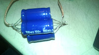
Now I can be tenacious but I can smell wasted time in this not to mention the fact that I didn't much trust those craptastic connections so I grabbed a large perfboard I had laying around as a spare from my arduino LED cube build. here is the link for the perfboard. So the game plan for today is to desolder those caps then mount each pack in a corner of the perfboard and work with them there. The question then becomes weather to mount the whole clock circuit like that or to leave the relays off the board and mount them similarly to the rest of the computer. I think either way mounting the capacitors like this will neaten things up nicely which is always a good thing.
Let's take a look at the physical relay's themselves as they're kind of neat. As you can see in the pictures the relays aren't overly large they measure about an inch and a half high 3/4 of an inch wide and 1 inch long there are a total of 14 pins on the bottom which are blade style for insertion into a socket and have a hole in the blade for easy solder application should that be the case. In our case I will be doing all of the prototyping with sockets for ease of assembly and testing purposes as well as building a nice test assembly for quick and easy pre installation testing. In the pictures I've included my watch for scale as the pictures included in the HP computer materials was a little hard on scale for me. Internally the relay is quite a marvel of efficient packaging and even includes an LED on the coil to indicate when it is
energized which should add a whole other dimension of blinky blinky to our build. It does give the benefit of potentially removing some indicators throughout the build and my first thought is to rid myself of the indicators for the clock circuit overall.
 The following pictures are labeled to show the individual sections on each relay. the full images of these are in the google doc as well as a few others that I took and left unlabeled. Once the clock is put together I will likely post a short video of it in action.
At this point we haven't had time to get much built and with the sockets coming not much will likely get built for a few more days but the capacitor packs will be getting assembled and the wiring planned I will also be working on the test rig and will post a schematic of that soon. On orders I looked deeper into the power supplies used in the HP computer and he uses a now defunct Radio Shack model that was a 13.8VDC 10 A CB radio supply a brief search through amazon found similar here. The supply is at the heart of this build and Harry Porter used 2 of these 10 A supplies and I will be as well though for the time being I have only ordered 1 for testing and prototyping. Originally I had planned on using an old computer power supply for the ease of adding a 5V line for the memory chip circuit. That plan may still be put to use as I have an 850W Corsair supply that should supply more than enough power for the whole shebang.
I know today was a big deviation from the theory of late but the physical components are what this will ultimately be about and as much time will be spent on that as on the understanding and planning of the operation of this computer. Monday will likely cover in depth the operation of the finished clock circuit. Likely with lots of build pictures and hopefully a video of it running too.
Well over a month in and finally some action I received the first 10 relay order Thursday and the 80 relay order form earlier this week Friday. So mental note. Fewer. Bigger. Orders. these coupled with the parts I already have and a quick trip to Radio Shack for some wire and quick and dirty switches has me poised to start building. The kids and I sat down to start work and 2 things became immediately clear 1 they wanted to know how it all worked in detail as bad as I did (good thing). 2 I have no idea how HP put those capacitors together the way he did because those leads leave no room for error with placement. Even with 2 sets of hands manning the iron and holding/positioning them just assembling 1 pack of 5 caps took the better part of 30 minutes.


Now I can be tenacious but I can smell wasted time in this not to mention the fact that I didn't much trust those craptastic connections so I grabbed a large perfboard I had laying around as a spare from my arduino LED cube build. here is the link for the perfboard. So the game plan for today is to desolder those caps then mount each pack in a corner of the perfboard and work with them there. The question then becomes weather to mount the whole clock circuit like that or to leave the relays off the board and mount them similarly to the rest of the computer. I think either way mounting the capacitors like this will neaten things up nicely which is always a good thing.
 |
| MY4 12DC coil 4PDT relay |
 |
| MY4 12DC coil 4PDT relay |
Let's take a look at the physical relay's themselves as they're kind of neat. As you can see in the pictures the relays aren't overly large they measure about an inch and a half high 3/4 of an inch wide and 1 inch long there are a total of 14 pins on the bottom which are blade style for insertion into a socket and have a hole in the blade for easy solder application should that be the case. In our case I will be doing all of the prototyping with sockets for ease of assembly and testing purposes as well as building a nice test assembly for quick and easy pre installation testing. In the pictures I've included my watch for scale as the pictures included in the HP computer materials was a little hard on scale for me. Internally the relay is quite a marvel of efficient packaging and even includes an LED on the coil to indicate when it is
energized which should add a whole other dimension of blinky blinky to our build. It does give the benefit of potentially removing some indicators throughout the build and my first thought is to rid myself of the indicators for the clock circuit overall.

 The following pictures are labeled to show the individual sections on each relay. the full images of these are in the google doc as well as a few others that I took and left unlabeled. Once the clock is put together I will likely post a short video of it in action.
At this point we haven't had time to get much built and with the sockets coming not much will likely get built for a few more days but the capacitor packs will be getting assembled and the wiring planned I will also be working on the test rig and will post a schematic of that soon. On orders I looked deeper into the power supplies used in the HP computer and he uses a now defunct Radio Shack model that was a 13.8VDC 10 A CB radio supply a brief search through amazon found similar here. The supply is at the heart of this build and Harry Porter used 2 of these 10 A supplies and I will be as well though for the time being I have only ordered 1 for testing and prototyping. Originally I had planned on using an old computer power supply for the ease of adding a 5V line for the memory chip circuit. That plan may still be put to use as I have an 850W Corsair supply that should supply more than enough power for the whole shebang.
I know today was a big deviation from the theory of late but the physical components are what this will ultimately be about and as much time will be spent on that as on the understanding and planning of the operation of this computer. Monday will likely cover in depth the operation of the finished clock circuit. Likely with lots of build pictures and hopefully a video of it running too.
Wednesday, March 2, 2016
Adding a right shift register
Day 29
I am considering adding constant and circular shift right to my function set this will mean adding some complexity to the 3-8 decoder as it would then need at least 11 total outputs but adding 1 more bit to the input line will give me up to 16 total instructions so I am thinking on more instructions to add to make this change worth the effort. The constant would add another memory register but could be completely switch operated to save components, more on that Saturday.
The right shift function itself could be easily called by inserting a pair of relays into the left shift data stream before the shift and when enabled would simply reverse the order of the inputs. If you look at the schematic below it shows how I plan to implement this shift though the tagging makes it somewhat obfuscated. The b register inputs are on the right where they pass through the right shift enable circuit if the circuit is not enabled the NC contacts pass through the inputs in descending order where the most significant bit is shifted to the least significant spot and all others move up 1 place. If the relays are energized the order of inputs is reversed Shifting the least significant bit to the most significant place and all others moving down 1 place. The resulting outputs are placed into the left shift enable where if left shift is enabled then the bits simply pass through, if not the outputs are inverted again to match the data bus order. After this the resulting output will then have to go through yet another enable circuit that activates for either a left OR a right shift and a simple OR function will be added to the enable circuit to allow this and prevent feedback into the data bus.
 While this circuit adds 5 more relays minimum to the overall design I feel it also adds extra functionality that will save valuable compute cycles and saves the need for yet another data line set in this already large computer. the indicator lights will be placed at the input to the shift enable circuit to save the need for 8 extra lights. There will be either 1 or 2 lights to indicate which shift function is being called. I am as yet unsure if this will be a bi color LED, 2 separate indicators, or 1 indicator that is on for 1 shift or off for the other. That is a style call though so it can wait quite some time. I will be prototyping this circuit up ASAP.
Parts update, still no sign of anything from china but my capacitors and the first batch of indicators is out for delivery today. I also received shipping notification on the second larger batch of relays I ordered over the weekend so those should be here in a few weeks. I ended up making my purchase decision based on both the size of this order and the resultant per unit cost, fingers crossed it works out because that was quite a few relays. It did manage to get me below $2.50 each relay so I think I may try and do larger batch orders like that from now on.
I am considering adding constant and circular shift right to my function set this will mean adding some complexity to the 3-8 decoder as it would then need at least 11 total outputs but adding 1 more bit to the input line will give me up to 16 total instructions so I am thinking on more instructions to add to make this change worth the effort. The constant would add another memory register but could be completely switch operated to save components, more on that Saturday.
The right shift function itself could be easily called by inserting a pair of relays into the left shift data stream before the shift and when enabled would simply reverse the order of the inputs. If you look at the schematic below it shows how I plan to implement this shift though the tagging makes it somewhat obfuscated. The b register inputs are on the right where they pass through the right shift enable circuit if the circuit is not enabled the NC contacts pass through the inputs in descending order where the most significant bit is shifted to the least significant spot and all others move up 1 place. If the relays are energized the order of inputs is reversed Shifting the least significant bit to the most significant place and all others moving down 1 place. The resulting outputs are placed into the left shift enable where if left shift is enabled then the bits simply pass through, if not the outputs are inverted again to match the data bus order. After this the resulting output will then have to go through yet another enable circuit that activates for either a left OR a right shift and a simple OR function will be added to the enable circuit to allow this and prevent feedback into the data bus.

Parts update, still no sign of anything from china but my capacitors and the first batch of indicators is out for delivery today. I also received shipping notification on the second larger batch of relays I ordered over the weekend so those should be here in a few weeks. I ended up making my purchase decision based on both the size of this order and the resultant per unit cost, fingers crossed it works out because that was quite a few relays. It did manage to get me below $2.50 each relay so I think I may try and do larger batch orders like that from now on.
Subscribe to:
Comments (Atom)